


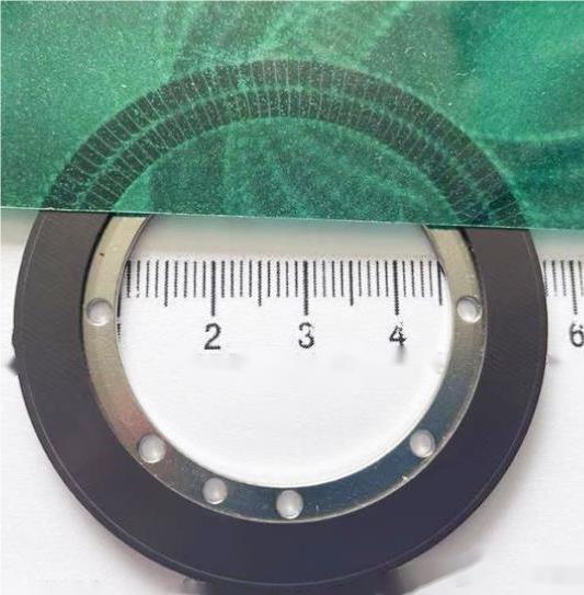
Our EMI rubber and conductive rubber pads combine electromagnetic wave absorption (8 – 30 GHz) with thermal conductivity (3.0 W/mK). Custom formulations in silicone, fluorosilicone, and EPDM base materials. UL 94 V-0 flame retardant. Serving 5G, automotive, medical, and industrial markets worldwide.
Overview
Our thermally conductive EMI absorbing pad is an advanced thermal interface material (TIM) engineered to solve two critical challenges in modern electronics: heat dissipation and electromagnetic interference (EMI). Built on a high-performance silicone rubber matrix, the material is loaded with precision-formulated thermally conductive ceramic fillers and magnetic absorbing particles to deliver reliable, long-term performance in demanding applications.
Unlike conventional thermal pads or standalone EMI shielding solutions that address only one function, this dual-purpose EMC absorbing material integrates both capabilities into a single compressible layer — reducing component count, streamlining assembly, and saving valuable space in densely packed designs. It provides effective RF absorption across a broad frequency spectrum from 8 GHz to 30 GHz, covering critical 5G mmWave bands, while maintaining a thermal conductivity of 3.0 W/mK for efficient heat transfer.
The pad features an inherently tacky surface on both sides, eliminating the need for additional adhesive layers or mechanical fasteners during assembly. Its low Shore 00 hardness (30–55) ensures excellent conformability and gap-filling capability under minimal compression, accommodating surface roughness and tolerance variations without imparting excessive mechanical stress on sensitive components. With a UL 94 V-0 flame retardancy rating and an operating temperature window of -40°C to +160°C, this silicone thermal pad meets the reliability requirements of telecommunications infrastructure, automotive under-hood environments, and outdoor wireless equipment.
Key Features
Typical Applications
This thermally conductive EMI absorber is designed for high-frequency electronic systems where both thermal management and electromagnetic compatibility (EMC) are critical design requirements. Common use cases include:
Additional applications: wireless charging modules, mmWave antenna arrays, satellite communication terminals, power amplifiers, FPGA / ASIC thermal management, LiDAR sensors, infotainment head units, and industrial embedded controllers.
Why Choose Our EMI Thermal Pad
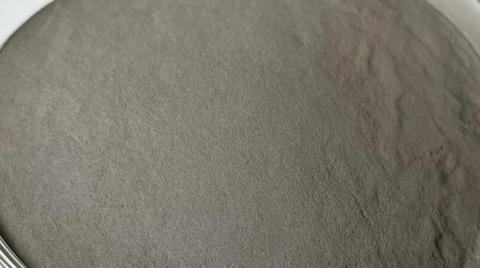
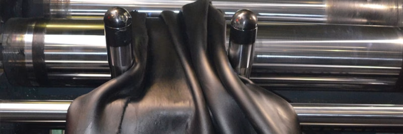
Engineers selecting a thermal gap filler with EMI absorption face trade-offs between thermal performance, electromagnetic attenuation, mechanical compliance, and cost. Our material is optimized across all four dimensions:
- Material development capability — in-house formulation expertise allows us to adjust thermal conductivity, hardness, and absorption band to match your specific design targets, rather than forcing your design to fit an off-the-shelf product.
- Broadband RF absorption — effective from 8 GHz through 30 GHz and beyond, covering the full 5G FR2 spectrum (24.25–52.6 GHz), automotive radar (24 GHz and 77 GHz), and m��Ku/m��Ka-band satellite links.
- Low oil bleed (<1%) — minimal siloxane outgassing ensures long-term stability without contaminating optical surfaces or connector contacts in adjacent subsystems.
- Die-cut ready — supplied in standard 200 × 300 mm sheets and compatible with high-speed rotary and flatbed die-cutting for complex geometries, including holes, slots, and irregular perimeters with tight tolerances.
Recommended Frequency Range
Effective Absorption Range
8 – 30 GHz
Covers 5G FR2 bands (n257 / n258 / n261), mmWave radar (24 / 77 GHz), m��Ku/m��Ka-band satellite communications, and other high-frequency applications
Technical Specifications
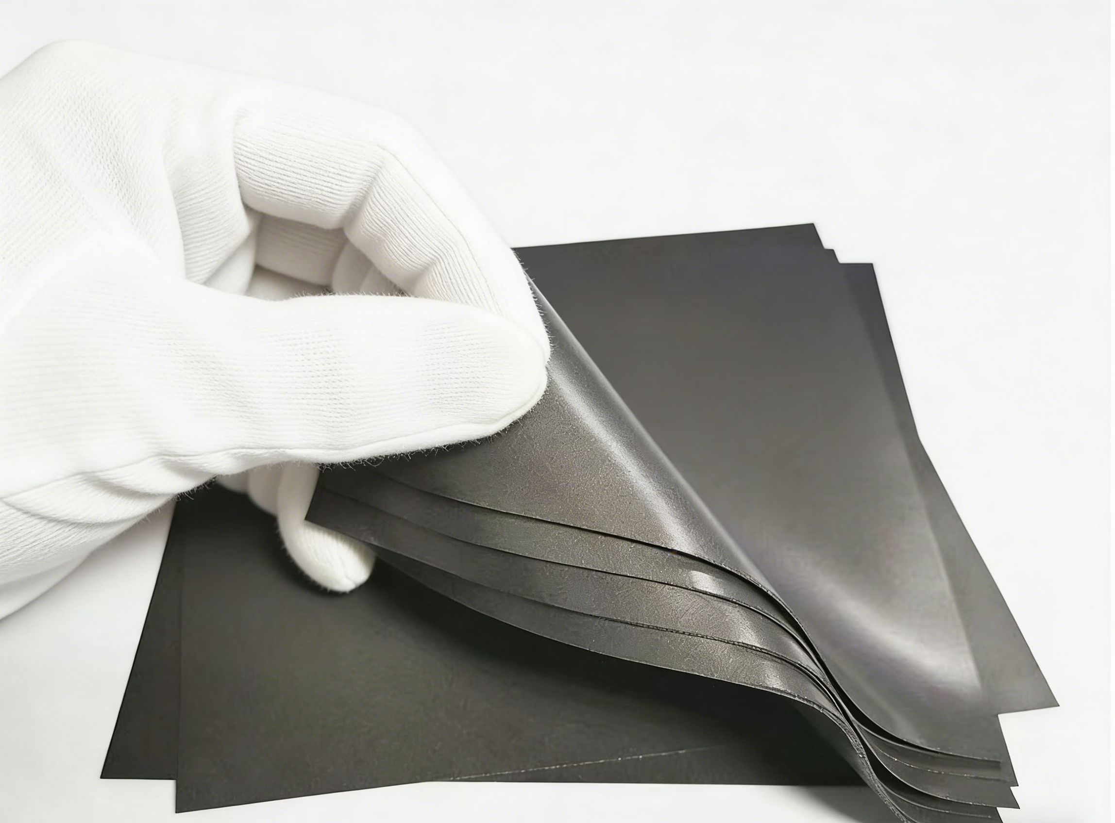
General Specifications
| Property | Specification | Test Instrument | Test Method |
|---|---|---|---|
| Color | Gray-Black | – | Visual |
| Thickness | 0.5 – 3.0 mm (standard); custom available | Digital Caliper | – |
| Hardness | 60 – 70 Shore A | Durometer | GB/T 531.1-2008 |
| Thermal Conductivity | 3.0 W/mK | Hot Disk TPS 2500S | ISO 22007-2 |
| Volume Resistivity | 0.004 – 10 Ohm.cm | 4-Point Probe | GB/T 36763-2018 |
| EMI Absorption Range | 8 – 30 GHz | Vector Network Analyzer | GB/T 36763-2018 |
| Flame Retardant | UL 94 V-0 (standard); HB (conductive) | Flame Chamber | UL 94 |
| Operating Temperature | -40C to +160C | Environmental Chamber | – |
| Surface Tack | Inherently tacky | – | – |
| Density | 1.3 – 3.5 g/cm3 | Analytical Balance | GB/T 533-2008 |
| Tensile Strength | 1.5 – 6.5 MPa | Universal Testing Machine | GB/T 528-2009 |
| Elongation at Break | 90% – 300% | Universal Testing Machine | GB/T 528-2009 |
| Compression Set | 25% – 68% | Compression Fixture | GB/T 7759.1-2015 |
| RoHS | YES | – | – |
OBT-CEA Series – Multi-Material Conductive Rubber
Nickel-graphite, silver-glass, silver-aluminum, silver-copper, nickel-aluminum formulations in silicone.
| Property | OBT-CEA6701 | OBT-CEA1801 | OBT-CEA1501 | OBT-CEA1301 | OBT-CEA6501 |
|---|---|---|---|---|---|
| Conductive Filler | Ni/Graphite | Ag/Glass | Ag/Al | Ag/Cu | Ni/Al |
| Color | Gray-Black | Beige | Blue/Beige | Brown | Gray-Black |
| Vol Resistivity | 0.1 | 0.01 | 0.008 | 0.004 | 0.15 |
| Density (g/cm3) | 2.0 | 1.9 | 2.1 | 3.5 | 3.5 |
| Hardness (Shore A) | 70 | 70 | 70 | 70 | 70 |
| Tensile (MPa) | 2.0 | 2.0 | 2.0 | 2.0 | 1.5 |
| Elongation | 100% | 90-200% | 100-200% | 100-300% | 100% |
| Tear (kN/m) | 6.2 | 5.3 | 5.3 | 7.0 | 7.0 |
| Max Temp (degC) | 150 | 160 | 160 | 125 | 125 |
| Shield 2GHz (dB) | 110 | 90 | 115 | 120 | 100 |
| Shield 10GHz (dB) | 100 | 80 | 105 | 120 | 85 |
| Shield 18GHz (dB) | 100 | 80 | 100 | 115 | 67 |
| Flame / RoHS | HB / YES | HB / YES | HB / YES | HB / YES | HB / YES |
Customization & Inquiries
With in-house material R&D and formulation capabilities, we can tailor this thermally conductive EMI absorbing pad to your exact specifications — including custom thicknesses from 0.5 to 5.0 mm, complex die-cut geometries with tight tolerances, mixed-size sheet formats, and roll packaging compatible with automated pick-and-place assembly. Whether you need small-batch samples for design validation and EMC pre-compliance testing, or full-scale production volumes with consistent lot-to-lot performance, our team is equipped to support your project from concept to mass production.
Contact our sales engineers today to discuss your thermal management and EMI shielding requirements. You will receive a technical proposal with application-specific recommendations and a competitive quotation within 24 hours. Free samples are available for qualified projects.
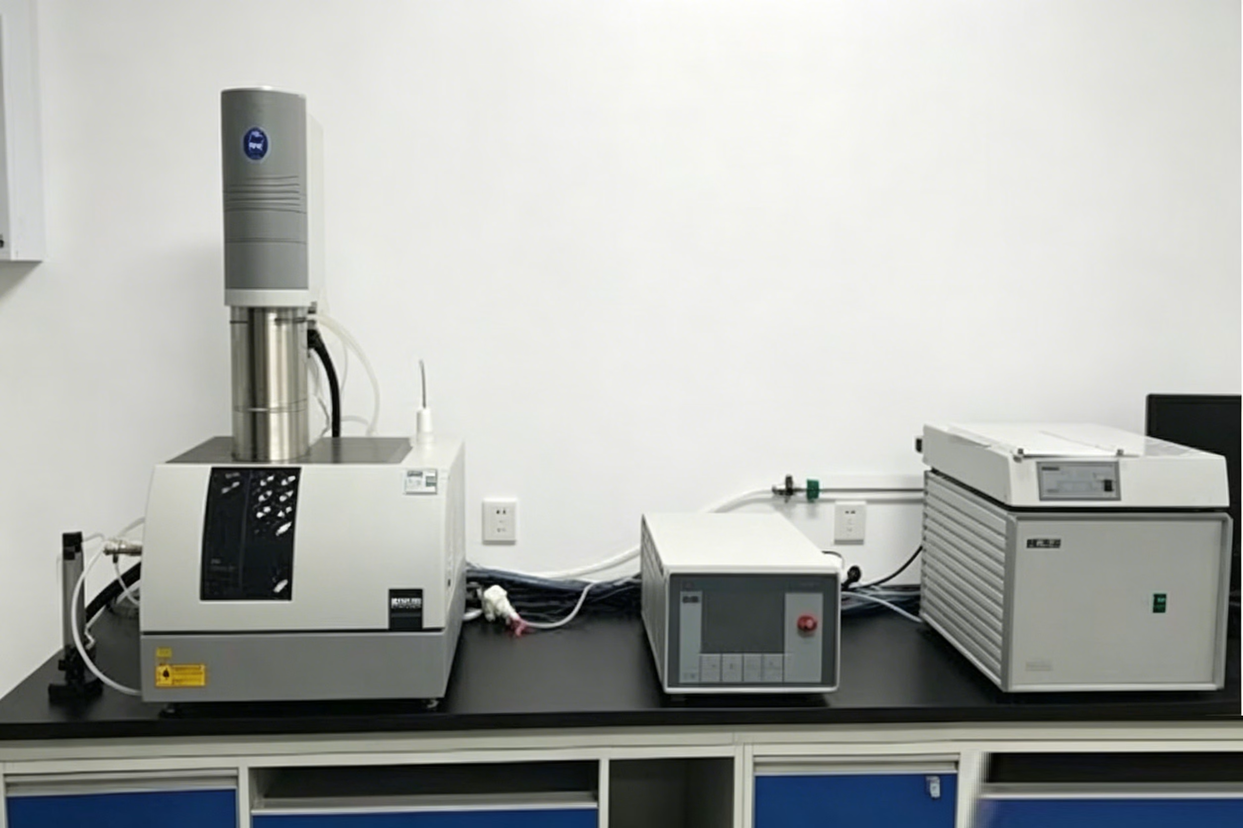
LW-9389 Thermal Conductivity Tester — ASTM D 5470 compliant
Get Started with OBT Conductive Rubber
Whether you need a standard EMI absorbing pad or a fully custom conductive rubber formulation, our in-house R&D team can help. We offer:
- Free technical consultation �� tell us your frequency range, thermal requirements, and mechanical constraints
- Custom sample service �� prototype gaskets, sheets, or die-cut parts delivered in 1-2 weeks
- Volume production with 100% inspection �� ISO-certified manufacturing
Contact Us Now Most inquiries receive a detailed response within 24 hours.
Frequently Asked Questions
Q1: What is a thermally conductive EMI absorbing pad?
A thermally conductive EMI absorbing pad — also referred to as a thermal EMI absorber, EMC gap filler, or RF absorbing thermal pad — is a composite sheet material that simultaneously transfers heat away from electronic components and attenuates unwanted electromagnetic interference. It combines thermally conductive ceramic fillers (for heat conduction) with magnetic or dielectric lossy fillers (for RF absorption) in a compressible silicone elastomer matrix, providing both thermal management and EMI shielding in a single layer.
Q2: What frequency range does this material cover?
The pad is optimized for broadband absorption from 8 GHz to 30 GHz, with measurable attenuation extending beyond this range. This covers the key 5G mmWave FR2 bands (n257: 26.5–29.5 GHz, n258: 24.25–27.5 GHz, n261: 27.5–28.35 GHz), 24 GHz automotive radar, and m��Ku/m��Ka-band satellite downlinks. For applications requiring absorption at lower frequencies (e.g., sub-6 GHz 5G, 2.4 GHz / 5 GHz Wi-Fi), please contact us for alternative formulations with shifted absorption bands.
Q3: Can this pad replace a traditional thermal pad plus a separate EMI shield?
Yes — that is the primary design objective of this material. By consolidating thermal conductivity and EMI absorption into one layer, you eliminate the cost, thickness, and assembly complexity of using a separate thermal gap filler and conductive EMI gasket or board-level shield. This is especially valuable in space-constrained designs such as smartphones, small cells, automotive radar modules, and wearable electronics where every fraction of a millimeter counts.
Q4: How should this pad be stored and handled?
Store in a cool, dry environment at 15–30°C with relative humidity below 70% RH. m��Keep the material in its original sealed packaging away from direct sunlight and UV exposure. Under these conditions the shelf life is 12 months from the date of shipment. Once removed from packaging, the tacky surface may attract dust — handle with clean gloves in an ESD-safe assembly area. The pad does not require refrigeration or curing.
Q5: Do you offer custom thicknesses, colors, or formulations?
Absolutely. We have in-house material development and compounding capabilities, which means we can adjust the formulation to meet your exact specifications. Common customizations include: non-standard thicknesses (0.3 mm up to 5.0 mm), modified thermal conductivity (1.5–5.0 W/m·m��K), shifted absorption frequency bands, different Shore hardness ranges, specific color requirements, and enhanced dielectric breakdown voltage for high-voltage applications. Contact our engineering team with your target specifications and we will develop a tailored solution.
Q6: Is this material compatible with automated assembly processes?
Yes. The pad is die-cut compatible and can be supplied as individual pieces on kiss-cut liner tape suitable for vacuum pick-up nozzles.
Q7: What is the minimum order quantity (MOQ) and typical lead time?
For prototype and evaluation samples, we offer small quantities (as few as 5–10 sheets) with a lead time of 3–5 working days. For production orders, standard lead time is 2–3 weeks depending on thickness, die-cut complexity, and order volume. We maintain buffer stock of standard thicknesses (0.5, 1.0, 1.5, 2.0, 2.5, 3.0 mm) to support urgent requirements. Contact our sales team for a current MOQ and delivery schedule based on your specific configuration.
* The above data represent typical laboratory values measured under controlled conditions and are not guaranteed for every production batch. Specifications are subject to change without notice. Custom thicknesses, sheet sizes, die-cut geometries, and formulation adjustments are available upon request — please contact our sales team for a detailed datasheet and quotation. * Recommended storage conditions: 15–30°C, <70% RH, away from direct light, in original sealed packaging. Shelf life: 12 months from date of shipment. Once opened, use within 60 days for best performance.


